- 您现在的位置:买卖IC网 > Sheet目录1903 > AT89C51ID2-RLRIM (Atmel)IC MCU FLASH 8051 64K 5V 44-VQFP
32
AT89C51ID2
4289C–8051–11/05
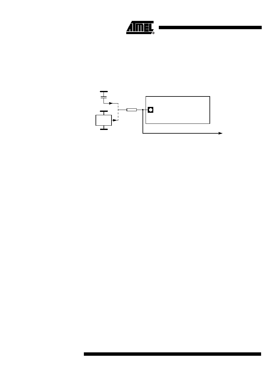
Reset Output
As detailed in Section “Hardware Watchdog Timer”, page 107, the WDT generates a 96-
clock period pulse on the RST pin. In order to properly propagate this pulse to the rest of
the application in case of external capacitor or power-supply supervisor circuit, a 1 k
Ω
resistor must be added as shown Figure 9.
Figure 9. Recommended Reset Output Schematic
RST
VDD
+
VSS
VDD
RST
1K
To other
on-board
circuitry
AT89C51ID2
发布紧急采购,3分钟左右您将得到回复。
相关PDF资料
AT89C51RC-24PU
IC MCU 32K FLASH 24MHZ 40-DIP
AT89C51RC2-RLRIL
IC MCU FLASH 8051 32K 3V 44-VQFP
AT89C51RE2-SLRUM
MCU 8051 128K FLASH 44-PLCC
AT89C51SND1C-7HTUL
IC MCU 64KB FLASH MEM 81-CBGA
AT89C51SND2C-7FTUL
IC 8051 MCU FLASH 64K MP3 100BGA
AT89C52-24PI
IC MICRO CTRL 24MHZ 40DIP
AT89C55WD-24AU
IC 8051 MCU FLASH 20K 44TQFP
AT89EB5114-TGSIL
IC 8051 MCU FLASH 4K 20SOIC
相关代理商/技术参数
AT89C51ID2-RLRUM
功能描述:8位微控制器 -MCU C51ID2 64K FLASH 32KHz 3-5.5V RoHS:否 制造商:Silicon Labs 核心:8051 处理器系列:C8051F39x 数据总线宽度:8 bit 最大时钟频率:50 MHz 程序存储器大小:16 KB 数据 RAM 大小:1 KB 片上 ADC:Yes 工作电源电压:1.8 V to 3.6 V 工作温度范围:- 40 C to + 105 C 封装 / 箱体:QFN-20 安装风格:SMD/SMT
AT89C51ID2-RLTIM
功能描述:IC 8051 MCU FLASH 64K 44VQFP RoHS:否 类别:集成电路 (IC) >> 嵌入式 - 微控制器, 系列:89C 标准包装:9 系列:87C 核心处理器:8051 芯体尺寸:8-位 速度:40/20MHz 连通性:UART/USART 外围设备:POR,WDT 输入/输出数:32 程序存储器容量:32KB(32K x 8) 程序存储器类型:OTP EEPROM 大小:- RAM 容量:256 x 8 电压 - 电源 (Vcc/Vdd):4.5 V ~ 5.5 V 数据转换器:- 振荡器型:内部 工作温度:0°C ~ 70°C 封装/外壳:40-DIP(0.600",15.24mm) 包装:管件
AT89C51ID2-RLTUM
功能描述:8位微控制器 -MCU C51ID2 64K FLASH 32KHz 3-5.5V RoHS:否 制造商:Silicon Labs 核心:8051 处理器系列:C8051F39x 数据总线宽度:8 bit 最大时钟频率:50 MHz 程序存储器大小:16 KB 数据 RAM 大小:1 KB 片上 ADC:Yes 工作电源电压:1.8 V to 3.6 V 工作温度范围:- 40 C to + 105 C 封装 / 箱体:QFN-20 安装风格:SMD/SMT
AT89C51ID2-SLRIM
功能描述:IC MCU FLASH 8051 64K 5V 44-PLCC RoHS:否 类别:集成电路 (IC) >> 嵌入式 - 微控制器, 系列:89C 标准包装:1,500 系列:AVR® ATtiny 核心处理器:AVR 芯体尺寸:8-位 速度:16MHz 连通性:I²C,LIN,SPI,UART/USART,USI 外围设备:欠压检测/复位,POR,PWM,温度传感器,WDT 输入/输出数:16 程序存储器容量:8KB(4K x 16) 程序存储器类型:闪存 EEPROM 大小:512 x 8 RAM 容量:512 x 8 电压 - 电源 (Vcc/Vdd):2.7 V ~ 5.5 V 数据转换器:A/D 11x10b 振荡器型:内部 工作温度:-40°C ~ 125°C 封装/外壳:20-SOIC(0.295",7.50mm 宽) 包装:带卷 (TR)
AT89C51ID2-SLRUM
功能描述:8位微控制器 -MCU C51ID2 64K FLASH TWI 32KHz 5V RoHS:否 制造商:Silicon Labs 核心:8051 处理器系列:C8051F39x 数据总线宽度:8 bit 最大时钟频率:50 MHz 程序存储器大小:16 KB 数据 RAM 大小:1 KB 片上 ADC:Yes 工作电源电压:1.8 V to 3.6 V 工作温度范围:- 40 C to + 105 C 封装 / 箱体:QFN-20 安装风格:SMD/SMT
AT89C51ID2-SLSIM
制造商:ATMEL 制造商全称:ATMEL Corporation 功能描述:8-bit Flash Microcontroller
AT89C51ID2-SLSUM
功能描述:8位微控制器 -MCU 64K FLASH 32KHz 3.5-5V Ind. RoHS:否 制造商:Silicon Labs 核心:8051 处理器系列:C8051F39x 数据总线宽度:8 bit 最大时钟频率:50 MHz 程序存储器大小:16 KB 数据 RAM 大小:1 KB 片上 ADC:Yes 工作电源电压:1.8 V to 3.6 V 工作温度范围:- 40 C to + 105 C 封装 / 箱体:QFN-20 安装风格:SMD/SMT
AT89C51ID2-SMSIM
制造商:ATMEL 制造商全称:ATMEL Corporation 功能描述:8-bit Flash Microcontroller